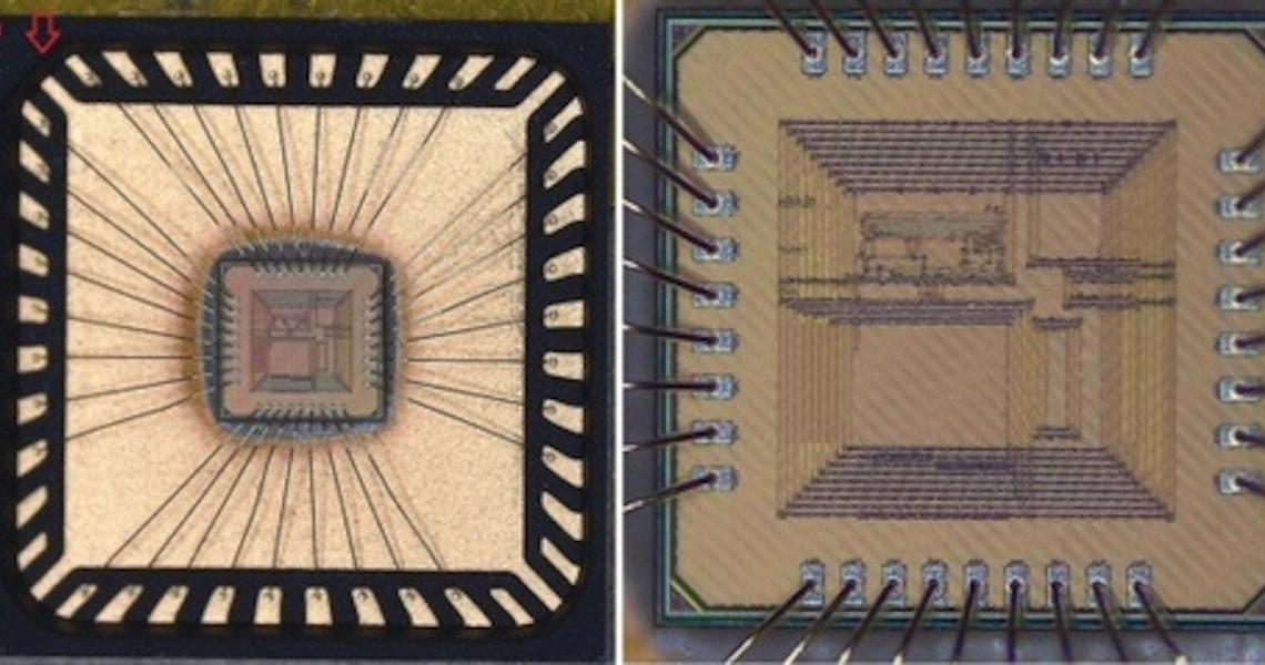
Artificial Intelligence Pushes Internet Device CPUs Outside the Box

The energy usage of 75 billion Internet-connected devices could be reduced 1,000-fold if those devices could do more thinking for themselves rather than constantly asking cloud servers for help, computer engineering Assistant Professor Shaahin Angizi believes.
Artificial intelligence will be the application driving this need in such devices by the second half of the 2020s, not just in devices like Amazon Alexa but in everyday objects at home, work, your car and in industry.
So instead of focusing on cloud or network innovation to save energy, and also to make devices respond faster, Angizi believes the answer is to make new kinds of computer chips that turn traditional architecture upside-down. He began his teaching career last fall and is already armed with a pair of National Science Foundation grants for $300,000 and $280,000, to study what experts call in-memory computing and in-sensor computing, respectively.
In traditional CPUs, there are separate areas for processing and memory. It's mostly been that way since Charles Babbage began designing a mechanical computer called the Analytical Engine in 1837, with sections that he called the mill and store, named for Victorian-era metaphors. The same format for electronic computers picked up the misnomer Von Neumann architecture in the 1940s, named for the mathematician who advocated the idea that others of his time pioneered.
Angizi is part of a trend among engineers and computer scientists who see value in changing the layout. Rather than performing computation inside the main CPU, they assert, you can instead do the Boolean logic inside cache memory, or even directly inside physical sensors with carefully placed transistors, which would be faster and electrically economical compared to waiting for a device-to-cloud-to-server connection, and back again.
The team's in-memory design is faster than most others, and their in-sensor design could save data for 10 years, vs. just a few years for competitive designs. Angizi described a hypothetical application in healthcare, where an emergency room worker could scan a patient's wound with a handheld device that would use in-sensor computing to evaluate the image and in-memory computing to perform artificial intelligence on possible actions to take.
"The greatest challenges in the semiconductor industry right now are the power wall and the memory wall. The problem that is less explored is what we have at the architecture level," said Angizi, whose team in NJIT's Advanced Circuit-to-Architecture Design Laboratory have already applied for patents and developed some of the field's most sophisticated working prototypes.
Angizi said his collaborators outside of NJIT include experts at Arizona State University, State University of New York-Albany and University of Nebraska-Lincoln. In a recent collaboration with ASU, they presented an ultra-fast, in-memory computing prototype at 65 nanometers this semester to the IEEE 52nd European Solid-State Device Research Conference, in Milan, Italy.